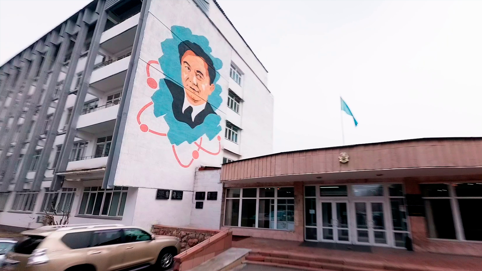
Institute of Physics and Technology
The Institute of Physics and Technology was established by the Resolution of the Council of Ministers of the Kazakh SSR dated December 27, 1990 No. 535 "On the organization of the Physics and Technology Institute of the Academy of Sciences of the Kazakh SSR".
Since 2015, the sole founder is NAO KazNTU. The Institute is located in a picturesque suburb of Almaty, the Alatau microdistrict.
Leading scientists who made world-class discoveries in the field of elementary particle physics and magnetic resonance EPR tomography contributed to the history of the Institute and Kazakhstani science.
The Institute defines the goal of becoming a center for applied and fundamental scientific research due to a high concentration of talent, an abundance of resources, effective management to create favorable conditions for the formation of scientific groundwork, obtaining competitive results, their implementation and publication in leading scientific journals with a high impact factor, which inspire, attract and retain young scientists, high-level scientists.
Currently, PTI LLP is one of the leading scientific centers in the field of solid state and semiconductor physics, materials science, nanoscience and nanotechnology, high energy physics and cosmic rays, has 8 scientific laboratories that have a scientific and technological infrastructure for fundamental and applied research, which conducts advanced research, development and design work.
The Kazakh scientific school in the field of condensed matter physics and ion-beam modification of materials created at the Physicotechnical Institute is generally recognized.
The Institute of Physics and Technology has accumulated a large volume of data on nuclear interactions obtained at accelerators of the world's largest scientific centers.
There are data on the interactions of: heavy Pb and medium S nuclei at energies of 150 GeV and 200 GeV per nucleon, heavy Au and medium Si nuclei at energies of 11 GeV and 14 GeV per nucleon, medium nuclei - C, O, S, Si, at energies of 3.7 GeV per nucleon.
Creation of the necessary technological infrastructure for the implementation of programs and projects in the direction of "Nanotechnology and new materials"
Creation of a modern hardware base for experimental methods for the synthesis of nanoscale structures - molecular beam epitaxy, vapor-phase epitaxy, ion-beam synthesis, ion implantation, sol-gel technology
Development of hardware and analytical tools for analyzing the properties of nanoscale objects, nanostructures and clusters, for targeted modification of material properties
Development of globally competitive scientific products and commercial technologies for the synthesis of nanostructures for a wide range of applications based on a wide class of substances
Development of metallothermic, pyrometallurgical, chemical and crystallization technologies for obtaining and purifying semiconductor materials for use in micro- and nanoelectronics, photovoltaics and other fields
The effect of hydrogen passivation of radiation defects in crystalline silicon, which consists of removing deep levels from the forbidden zone that determine the electronic properties of the material, has been discovered and studied.
A new phenomenon of hydrogen-accelerated formation of nanoclusters in silicon consisting of vacancies, interstitial atoms and impurity atoms has been discovered and studied . The use of this effect opens up a new direction of self-organized synthesis of nanostructures.
A series of defect-impurity centers in silicon have been discovered, which, according to the world classification, have received the name Almaty 1,……19. It should be noted that in terms of the number of discovered EPR centers, this is approximately 10% of the total number and is the third indicator in the world after the laboratories of Professor George Watkins (Albany, USA) and Professor Ammerlaan (Amsterdam, Netherlands), leaving far behind (four EPR centers each) world-famous scientific centers such as the A.F. Ioffe Physical-Technical Institute of the Russian Academy of Sciences (St. Petersburg) and the Institute of Semiconductor Physics of the Siberian Branch of the Russian Academy of Sciences (Novosibirsk).
A unique high-current accelerator of ultra-low energy ions has been developed, the authors of which hold patents in the USA. Using this accelerator, the physical principles of silicon doping by low-energy ion implantation with atomic and molecular beams, ion-plasma technology for manufacturing devices and synthesis of coatings with valuable properties for practical use have been developed. A know-how technology for manufacturing semiconductor radiation detectors with parameters that are record-breaking to date has been developed. These detectors have worked without degradation of parameters for more than twenty thousand hours on board aircraft in outer space.
An isolated self-interstitial atom and a number of radiation defects in silicon, including those with properties of bi- and metastability, have been discovered and identified (Advances in Physical Sciences, 2000, pp. 143-155).
A technology has been developed for producing semiconductor silicon and gaseous monosilane (SiH4 molecule) by processing silicate slags (Preliminary patents of the Republic of Kazakhstan No. 17865 and No. 17866. Patent No. 17865 also received a positive decision from the International Patent Agency).
The physical principles of silicon doping by the method of low-energy ion implantation with atomic and molecular beams, ion-plasma technology for the manufacture of devices and the synthesis of coatings with properties valuable for practical use have been developed (J. Rad. Eff. and DEf. In Solids, 1990. V.114, pp. 3-14).
An important aspect of the Physicotechnical Institute's activities is broad international scientific and technical cooperation: the Institute maintains contacts with many countries (USA, Germany, Japan, Russia, Saudi Arabia, etc.), which include about 70 research centers and universities, such as the European Organization for Nuclear Research CERN, Swansea University (United Kingdom), Joint Institute for Nuclear Research (Dubna, Russia), Skobeltsyn Research Institute of Nuclear Physics of Lomonosov Moscow State University (Russia), A.F. Ioffe Physical-Technical Institute of the Russian Academy of Sciences (Russia), Institute of Nuclear Physics of the Academy of Sciences of the Republic of Uzbekistan, Physicotechnical Institute of the Academy of Sciences of the Republic of Uzbekistan, and others.
In Kazakhstan alone, the Physicotechnical Institute cooperates with 50 research centers, universities, industrial enterprises and firms from various cities, such as Al-Farabi Kazakh National University, KazNU, Al-Farabi, UO Kazakh-German University in Almaty, PI National Laboratory Astana, NAO Karaganda Technical University, ZhenPU, and other organizations such as
Firma Balausa LLP, MK KazSilicon LLP, Electromanganets LLP, SEZ Pakr innovative technologies, and many others.
To get acquainted with the products, as well as current activities, we invite you to visit our Institute, where you can see real science, learn about our research and ask your questions to scientists of the old and new generations.
Please inform us in advance about a convenient time for you to visit:
+ 7 (727) 386 55 36 or by mail info@sci.kz